A xSignal runs between two pads (or nodes), but is identified as part of the net and follows the net topology design rule, which by default is Shortest.
To create an xSignal, select the required pads in the PCB panel then run the xSignals >> Create xSignals command. The dialog presents the selected pads, the start pad and the end pad.
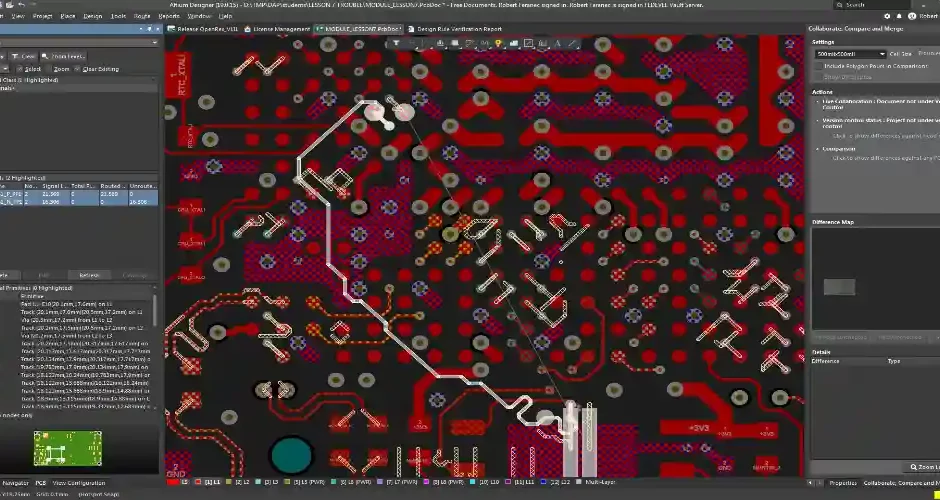
xSignal Analysis
An xSignal is a designer-defined path for a high-speed signal to travel between two nodes. These may be nodes within the same net, or two nodes in associated nets separated by a component. xSignals enable you to scope relevant design rules such as Length and Matched Length and apply interactive length tuning.
Using the xSignals Multi-Chip Wizard (Design >> xSignals > Run xSignals Wizard from the main menus or right-click in the PCB layout) you can quickly and easily identify and create xSignals for a range of different common interface and memory circuits. The Wizard takes a component-oriented approach to identifying potential xSignals, analyzing the paths from each source component to the designated components. This includes the route through any series passive components such as series termination resistors.
To begin, select a source component and its associated nets from the left panel of the dialog and select the destination components. When the analysis and creation process completes, all xSignals identified will be listed in the xSignals region of the dialog. By default all xSignals are enabled for creation – adjust this as required.
xSignal Routing
An xSignal is a designer-defined signal path between two nodes, which can be in the same or associated nets. An xSignal can be used to scope design rules such as Length and Matched Length, which are obeyed during design tasks such as interactive length tuning.
To create an xSignal, select the required source component and then choose a destination component. The software will attempt to identify any xSignals that exist between the chosen source components, including potential paths through series passive components and branch points.
If desired, you can also define a class for the xsignal opportunity. If you want to use a class, select the desired class from the list or enter a new name for a class in the text box at the bottom of the dialog. Click OK to complete the creation of the xSignal. The xSignal will now appear in the xSignals mode of the PCB panel. You can also use the xSignals mode of the panel to edit existing xSignals.
xSignal Design
A xSignal is a designer-defined signal path between two nodes, either in the same net or in associated nets separated by a component. This allows for the definition of matched length design rules to be scoped on the xSignal itself and obeyed during interactive length tuning.
To create xSignals use the new xSignal Multi-Chip Wizard – select a source component, its nets and then choose the destination components — the Wizard automatically analyzes all potential xSignal paths between the two components including those passed through series passive components such as series termination resistors. The xSignals are then created and available to be selected in the xSignal Mode of the PCB panel.
The xSignal mode of the PCB panel also supports the creation and selection of individual xSignals between pads, enabling you to quickly find the xSignal you want to edit and modify its settings. The xSignals are then automatically updated in the PCB Editor to reflect the changes you make.
xSignal Classes
xSignal Classes enable you to define and scope your own design rules to automatically obey for high-speed signal paths. These can include the Length and Matched Length design rules, as well as your own custom requirements.
The PCB panel’s middle region lists the xSignals you have created, or all of the xSignals in the design (All xSignals>). Select an xSignal to display it in the PCB design space as node pads joined by a thin line that represents the xSignal path.
The right-click context menu enables you to select the xSignal color, modify its visual representation in the PCB design space (Change xSignal Visualization), and delete it. The panel’s third region, xSignal Primitives, shows all the constituent elements (primitives) that make up the selected xSignal. This includes the total Pin/Package Length and routed length calculated from the sum of all placed track and arc segments, plus the vertical distance traversed by vias. It also displays the xSignal Margin, which is the difference between the actual xSignal length and the target signal length specified by applicable Length/Matched Length design rules.